- 您现在的位置:买卖IC网 > Sheet目录1201 > CDB5460AU (Cirrus Logic Inc)EVALUATION BOARD FOR CS5460A
�� �
�
�CS5460A�
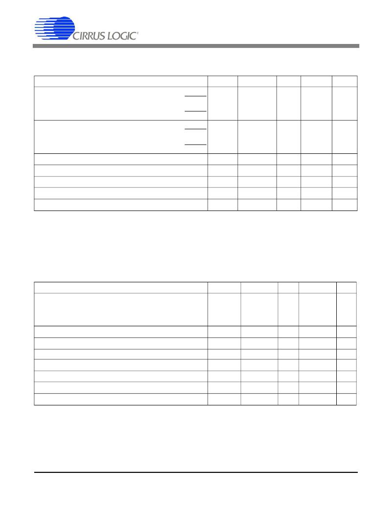
�3.3� V� DIGITAL� CHARACTERISTICS�
�(T� A� =� -40� °C� to� +85� °C;� VA+� =� 5� V� ±10%,� VD+� =� 3.3� V� ±10%;� VA-,� DGND� =� 0� V)� (See� Notes� 3,� 4,� and� 13)�
�Parameter�
�Symbol�
�Min�
�Typ�
�Max�
�Unit�
�High-Level� Input� Voltage�
�V� IH�
�All� Pins� Except� XIN,� XOUT,� SCLK,� and� RESET�
�XIN�
�SCLK� and� RESET�
�0.6� VD+�
�(VD+)� -� 0.5�
�0.8� ?� VD+�
�-�
�-�
�-�
�-�
�-�
�-�
�V�
�V�
�V�
�Low-Level� Input� Voltage�
�V� IL�
�All� Pins� Except� XIN,� XOUT,� SCLK,� and� RESET�
�XIN�
�SCLK� and� RESET�
�-�
�-�
�-�
�-�
�-�
�-�
�0.48�
�0.3�
�0.2� ?� VD+�
�V�
�V�
�V�
�High-Level� Output� Voltage� (except� XIN,� XOUT)� I� out� =� +5� mA�
�Low-Level� Output� Voltage� (except� XIN,� XOUT)� I� out� =� -5� mA�
�V� OH�
�V� OL�
�(VD+)� -� 1.0�
�-�
�-�
�-�
�-�
�0.4�
�V�
�V�
�Input� Leakage� Current�
�3-State� Leakage� Current�
�Digital� Output� Pin� Capacitance�
�(Note� 14)�
�I� in�
�I� OZ�
�C� out�
�-�
�-�
�-�
�±1�
�-�
�5�
�±10�
�±10�
�-�
�μA�
�μA�
�pF�
�Notes:� 15.� All� measurements� performed� under� static� conditions.�
�16.� If� VD+� =� 3� V� and� if� XIN� input� is� generated� using� crystal,� then� XIN� frequency� must� remain� between�
�2.5� MHz� -� 5.0� MHz.� If� using� oscillator,� full� XIN� frequency� range� is� available,� see� Switching�
��ABSOLUTE� MAXIMUM� RATINGS�
�(DGND� =� 0� V;� See� Note� 17)� WARNING:� Operation� at� or� beyond� these� limits� may� result� in� permanent� damage� to�
�the� device.� Normal� operation� is� not� guaranteed� at� these� extremes.�
�Parameter�
�Symbol�
�Min�
�Typ�
�Max�
�Unit�
�DC� Power� Supplies�
�(Notes� 18� and� 19)�
�Positive� Digital�
�Positive� Analog�
�Negative� Analog�
�Input� Current,� Any� Pin� Except� Supplies(Note� 20,� 21,� and� 22)�
�Output� Current�
�VD+�
�VA+�
�VA-�
�I� IN�
�I� OUT�
�-0.3�
�-0.3�
�+0.3�
�-�
�-�
�-�
�-�
�-�
�-�
�-�
�+6.0�
�+6.0�
�-6.0�
�±10�
�±25�
�V�
�V�
�V�
�mA�
�mA�
�Power� Dissipation�
�Analog� Input� Voltage�
�Digital� Input� Voltage�
�Ambient� Operating� Temperature�
�Storage� Temperature�
�(Note� 23)�
�All� Analog� Pins�
�All� Digital� Pins�
�P� D�
�V� INA�
�V� IND�
�T� A�
�T� stg�
�-�
�(VA-)� -� 0.3�
�DGND� -� 0.3�
�-40�
�-65�
�-�
�-�
�-�
�-�
�-�
�500�
�(VA+)� +� 0.3�
�(VD+)� +� 0.3�
�85�
�150�
�mW�
�V�
�V�
�°C�
�°C�
�Notes:� 17.�
�18.�
�19.�
�20.�
�21.�
�22.�
�23.�
�8�
�All� voltages� with� respect� to� ground.�
�VA+� and� VA-� must� satisfy� {(VA+)� -� (VA-)}� ?� +6.0� V.�
�VD+� and� VA-� must� satisfy� {(VD+)� -� (VA-)}� ?� +6.0� V.�
�Applies� to� all� pins� including� continuous� over-voltage� conditions� at� the� analog� input� (AIN)� pins.�
�Transient� current� of� up� to� 100� mA� will� not� cause� SCR� latch-up.�
�Maximum� DC� input� current� for� a� power� supply� pin� is� ±50� mA.�
�Total� power� dissipation,� including� all� input� currents� and� output� currents.�
�DS487F5�
�发布紧急采购,3分钟左右您将得到回复。
相关PDF资料
CDB5461AU
BOARD EVAL & SOFTWARE CS5461A
CDB5466U
BOARD EVAL & SOFTWARE CS5466 ADC
CDB5467U
BOARD EVAL FOR CS5467 ADC
CDB5560-2
DEV BOARD FOR CS5560 W/SE INPUT
CDB5571-2
DEV BOARD FOR CS5571 W/SE INPUT
CDB8422
BOARD EVAL FOR CS8422 RCVR
CDB8952T
BOARD EVAL FOR CS8952
CDCE906-706PERFEVM
EVAL MOD PERFORMANCE CDCE906/706
相关代理商/技术参数
CDB5460AU-Z
制造商:Cirrus Logic 功能描述:PB-FREEEVAL BOARD FOR CS5460 - Bulk
CDB5461
制造商:Cirrus Logic 功能描述:EVAL BD FOR CS5461 - Bulk
CDB5461A
功能描述:EVAL BOARD FOR CS5461 RoHS:否 类别:编程器,开发系统 >> 过时/停产零件编号 系列:- 标准包装:1 系列:- 类型:MCU 适用于相关产品:Freescale MC68HC908LJ/LK(80-QFP ZIF 插口) 所含物品:面板、缆线、软件、数据表和用户手册 其它名称:520-1035
CDB5461AU
功能描述:数据转换 IC 开发工具 Eval Bd Sngl-Phase Pow/Energy
RoHS:否 制造商:Texas Instruments 产品:Demonstration Kits 类型:ADC 工具用于评估:ADS130E08 接口类型:SPI 工作电源电压:- 6 V to + 6 V
CDB5461AU-Z
制造商:Cirrus Logic 功能描述:PB-FREEEVAL BOARD FOR CS5461 WITH USB - Bulk
CDB5462
制造商:Cirrus Logic 功能描述:EVAL BOARD FOR CS5462 - Bulk
CDB5463U
功能描述:数据转换 IC 开发工具 Eval Bd Sngl-Phase Pow/Energy
RoHS:否 制造商:Texas Instruments 产品:Demonstration Kits 类型:ADC 工具用于评估:ADS130E08 接口类型:SPI 工作电源电压:- 6 V to + 6 V
CDB5463U-Z
功能描述:EVAL BOARD USB FOR CS5463 RoHS:是 类别:编程器,开发系统 >> 评估板 - 模数转换器 (ADC) 系列:- 产品培训模块:Obsolescence Mitigation Program 标准包装:1 系列:- ADC 的数量:1 位数:12 采样率(每秒):94.4k 数据接口:USB 输入范围:±VREF/2 在以下条件下的电源(标准):- 工作温度:-40°C ~ 85°C 已用 IC / 零件:MAX11645 已供物品:板,软件